Category Archives: Test Equipment Repairs

For some, it is like solving crossword puzzles: fixing defective test equipment. Preferably, mid-70 to early 90s vintage.

Watkins-Johnson SE222-50 Backward Wave Oscillator: the magic helix

Recently, I got a Marconi Instruments Model 6651 RF Plug-in (26.5-40 GHz), for the 6600 sweep generator. These were basically the 1st generation sweep generators extending into the millimeter wave region.

A number of plug-ins were available, mostly based on Watkins-Johnson BWO (backward wave oscillators), which are a particular type of electron tube.

These sweepers were first introduced in the late 1960s, early 1970s. New plug-ins became available as development of BWOs and similar sources advanced.

I have no price list, but surely these items came at a hefty price tag in these early days, even not quite cheap today.

My unit had a pretty “new” 1990 date-code BWO, I expect, it had been replaced by its former university owner at least once, also the cables and connectors of the BWO looks newer compared to the rest of the plug-in. Because of their nature, the BWOs only have a limited life-time, a few 1000 hours at best.

There are numerous warning labels, because to focus the electron beam, a strong magnetic field is needed.

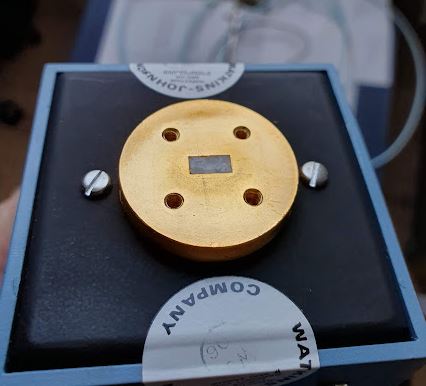
The output is a gold-plated waveguide flange, for Ku-band waveguides.

The general layout of a BWO: there is an electron gun, producing, in our case, a hollow electron beam, with the necessary heater, kathode, anode. Then, the helix, and the collector (which is basically at helix potential or a little bit higher, say, 100 volts higher. The helix voltage is quite high, for exmaple, 1~1.5 kV.

While there is no information from Watkins-Johnson available online for any of these devices, a lot can be learned from related Hewlett-Packard microwave sweeper plug-ins (8697A), where (arguable) the same or very similar BWO has been used (some HP units may use Varian BWOs).

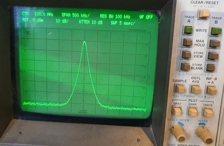
Unfortunately, after quite some effort with high voltages and pretty dangerous tests, it became clear that the tube barely gave some power. Maybe, because it had not been operated for a long time (some people and datasheets say that the BWO should be run at last once every 6 months, or similar, to preserve its function…).

But anyway, I have other, more stable and easy to use sources for this range, so I didn’t want to scrap the BWO without having a closer look at this. When do you normally get a chance to check out the secret workings of such marvelous devices!

First things first, hidden inside a heavy magnet, silicon rubber, and a waveguide coupler: the tube. A very mysterious piece of engineering, only a few companies ever mastered to produce these.

Also by the numbers and hand-writing, pretty clear that these units were all hand-made and assembled by engineers and highly skilled people.

The mount is all gold plated, a tapered wave guide eventually bent by 90°, so the microwave radian can be coupled from a small gap in the silver coating of the tube, to the outlet. This tube was meant to generate about 10 dBm.

The helix at the collector end.

You can see, the helix is kept centered by 3 glass (quarz?) rods, these rods are just held in place by the tension of the helix, but normally won’t move during operation and shipment. Surely, will all the glass-metal interfaces, mounts and connection points, it is no good idea to drop these units – some interfaces may break, or mis-align beyond repair. Furthermore, several Watts of powder will need to be dissipated, calling for a reasonably elaborate design of the mount not only to conduct the microwave radiation from the tube to the output, but also to dissipate the heat from the collector and helix.

All the high voltage socket part is embedded in two layers of silicon rubber. First they put some denser rubber around the socket to fix everything in place, probably run some tests, and then sealed it all by filling the further space with some pretty soft, highly filled silicon rubber. What they didn’t consider – the cable also has silicon isolation, and deteriorates in contact with other silicon materials. This may be one of the reasons for the unstable operation, because some wires were pretty close and the isolation seems very brittle.

Furthermore, I did some measurements of the critical parts, just in case I would even want to fabricate own BWOs, at least I have some working dimensions to start with.

The helix is normally made from flat molybdenum strip. At the bottom (gun end) it is mounted to a small ring. Scale is 210 px per 1 mm, in case you want to take dimensions…

A typical power supply – I am thinking about building a BWO power supply for some other old BWOs I have around (for other frequency regions), but it is fairly involved – the old design used high voltage 2 kV transformer with further high-voltage stable windings to provide the collector offset voltage, several expensive high voltage capacitors, and high voltage regulation vacuum tubes. I think it will be a good challenge for winter to build a 2 kV regulated and low-ripple power supply, solid state, probably with some series-connected MOSFETs.

Any of such future supplies will need a pretty special plug: heater voltage, anode and cathode voltages, helix voltage, collector voltage. At least I can go without any analog linearization voltage, if I manage to make the helix supply digitally controllable.

Inside the 6651 plug-in the BWO is connected to the board with some screw terminals. Seems to work well even at the high voltages. Surely there is no touch protection for these devices, just a few warnings not to get too close!

Olympia CD401 Tischrechner: a magnetic keyboard

This marvelous CD401 Nixie-Tube calculator came to me in pristine condition, from a friend, and including all the accessories and even the original power cord. Just that it has some small defects. Numbers 2 and 7 didn’t work, and some of the keys have mechanical issues. Noteworthy, this little calculator came from Japan, despite being branded Olympia (which is a German company no longer in existence), an made by Matsushita Electrics, also known as Panasonic, in the early 70s. It cost close to 1000 Deutschmarks, may be equivalent to a two week’s salary of an engineer at the time…

Someone had apparently tried to fix it before, using inappropriate tools and scratching some internals, and not taking care of proper alignment of the parts.

The non-reactive “2” could easily be traced by a continuity tester, a bad circuit trace (the grease seems to be slightly acidic and has some greenish discoloration in places – copper corrosion).

The trace would be easily fixed with a short wire and some solder. The other defect – maybe introduced by the earlier repair attempts, a broken reed switch. The keyboard as such is a remarkedly complex setup – each key has several metal and plastic parts, and a magnet that operates a reed switch. Clearly, this had been built to a certain standard of longevity at the time, an engineering tool rather than a “pocket calculator”.

I keep a box of reed switches as spares, so luckly found one that is a pretty exact fit of the original.

Some careful re-assembly, some cleaning of old grease, and the instrument can go for a test. Note that there is exposed mains voltage around the transformer – why didn’t they put some cover?? It is right open and exposed and will give you an electric shock when you touch it…

That’t finally the machine all fixed and in best working order, probably soon it will be 50 years old.

HP 3562A Signal Analyzer: a broken display and an easy fix

Recently, during some phase noise measurements, my 3562A failed. This instrument is an essential part of the noise test set, it is used for all frequency offsets up to 100 kHz, and as a signal/noise source (the 3562A has a fairly capable built-in noise source, signal source, etc.).
While the communication via GPIB went well and I could still complete the test job, the CRT went dark with no sign of life. I also have a second unit, with a LCD display, but the 3562A of the phase noise test set still has its original CRT. Let’s hope we can fix it because I don’t want to invest in a new LCD or anything for this purpose.

So I opened up the box (fortunately, it is accessible on top of the test set which is a stack of instruments, maybe 250 kgs of electronics), and did some checks. As it turns out, one of the rails of the CRT driver boards is down.

Some years back I had already replaced some tantalums, maybe some more of these have gone bad? So I cut some wires at suspicious capacitors – you can normally do this no problem, because the instrument will still function even with some buffer caps missing.

In fact, after the 3rd cut, the rail came back. The tantalum had a full short but no sign of smoke or heat, probably, because of various protection circuits of the power supply.

Replaced it with a similar electrolytic cap, probably this will do. It is a question of repair philosophy, should you replace all tantalums in such device, if you found two defective caps? I decided not to, because the fix every 5 years is easy enough, and there are just too many tantalums in it, moreover, I may break some contacts or cause issues with electrostatic discharge. For the current repair, I didn’t even remove the board, just cut the capacitor from the top and solder the spare back, from the top. As some old laser engineer told me once, the less you touch it, the better it will work. Sure enough, if the objective is to bring the unit back to the best state of reliability, it would be best just to replace the whole CRT by a new LCD assembly, or by a few 100 USD worth of KEMET high-rel tantalums and do a 5 hour solder and disassembly/assembly job…

HP 8569A Spectrum Analyzer: two mysterious resistors

Again, some repairs of a 8569A spectrum analyzer. This time, no problem at all with the front selectors and contacts that break all too often, but with the CRT showing only a defocused vertical line. Some probing around – the analyzer appears to be find but something wrong with the deflection circuit? This is on the A5 assembly, and with no extender board around, quite difficult to probe, and a bit dangerous because this assembly is using +120 VDC. Any short may damage the supply, and any touch may give you a shock. So better exercise some care. By soldering wires, I was able to trace the signal and it seemed to be OK up until to some of the last amplification stages of the X amplifier. Maybe something wrong with the transistors – no these are good. Probing around on the board, checking all values of components close-by: the 75k resistors (fairly large sized 0.5 Watt resistors) are high-resistance, both seemed to have failed at the same time – strange. Eventually, this is becoming a quite frequent failure, already the 5th case or so over the last few years of open high-ohmic, say, 100k and about, resistors that are subject to 100 V or similar “high voltage” usage.

With no suitable 75k resistors available, I went with a combination of 82k parallel to 880k, resulting in 75.01k, close enough. And the 82k resistors that need to carry most of the current are really good old low inductance transistors suitable for such 100 volts service.

The repair, it is not particularly beautiful, but it works and at no cost, with available parts. Finally, some hours of test to make sure there is nothing else at fault in this unit. All good, test passed.

Wavetek 172B Signal Generator: a heavy 00000000

This Wavetek has been part of an Army sale a while back, and I had used it for some project, but in recent years, it started to gather dust – it is a nice units but pretty heavy and I don’t want to hurt my back.
When I switched it on recently, it showed all “0000000”. The keypad is responsive and a beep sounds with any key pressed, but there is no reaction or output. Sure this can be fixed but I am not a Wavetek expert and all hands full with large gardens and other projects. So I sold the Wavetek to Ulrich Prinz DC3AX who kindly fixed it and shared the repair pictures and details below. Also I have the EPROMs archived in the Manuals Archive in case you need it.

Turns out that the keyboard has an independent processor, but the main CPU board is not initializing properly, normally, it needs to send a string “Wavetek 172B” to the display with self test completed, but the CPU doesn’t do anything.

The sockets on these boards are nowhere near Hewlett Packard quality, but single spring low cost IC sockets that are prone to aging and contact issues. The most critical ones around the PROMs were replace with precision contact IC sockets.

M2114 4k static RAMs, these are known to fail at times, so they were replaced.

Finally, a test, and it boots up and runs through the self test no issues. A marvelous repair because CPU boards can be tricky to fix – let’s hope for long and trouble-free service of the unit at its new owner!

HP 4140B pA Meter/DC Voltage Source: some incorrect assumptions, but finally, a repair

Shortly prior to my departure from Japan I started repair of a HP 4140B. A very desirable instrument for semiconductor characterization. The issue remained that output “A” didn’t provide correct voltages, probably due to some issues in the amplifier.
Two month later, I have returned to Germany, and a spare LF256 J-FET opamp had arrived, so I thought it would be a quick fix – but to no avail.

Fitting the LF256 to the board – I usually leave some part of the old wire in the Teflon isolator, because I want to avoid soldering/melting the solder in the Teflon part – it is all difficult to clean up afterwards, so I prefer to solder the new part to some leftover wire, rather than contaminating the isolator.

But- with the new opamp installed, same symptom, no proper output, current limit function of channel A blinking, but the input of the opamp is good. So it must be something else down the chain. Another look at the schematic…

There is an analog switch, followed by a discrete linear amplifier with a dual J-FET input stage.
After some study of the analog switch (cutting a trace and checking it), the switch appears fine. Next in line, the dual J-FET, and in fact, this is dead – found it by measuring the E-B and C-B transition voltages with a diode tester (instrument powdered down and board removed!!), and the transistor around the FET shows largely different values compared to the working B channel. It is 1855-0049 HP part, available in some single piece quantities but expensive!

Looks still shiny and new, but it isn’t working.

Studying some NSN databases, found at least some data of this part, which had been manufactured in equivalent versions by some other manufacturers as well, probably in the 1970s.

It is a rather not so special depletion n-type J-FET. But it is a dual FET part, and while single J-FETs are no problem to get, dual FETs are rare specimens.

Even in their long past days, these didn’t come cheap… maybe something like 40 EUR a piece in today’s money.

So we need to do further study, and there are essentially two kinds of dual FETs – some that have a specially made dual die, with both FETs on one chip and coupled in various ways to keep them from drifting apart with temperature, etc., and the other kind, which is merely just two reasonably matched separate FETs in one case, for convenience more than anything (and for thermal match).

Screening through my inventory I found these 2N5457 FETs which have pretty similar electrical characteristics, in particular, zero-gate-voltage currents.

The parts I have are all quite uniform so there is no need to select a special pair.

With such replacement with similar parts, rather than identical parts, I think it is a good idea to take no risk, so I took the B-channel dual FET and transplanted it to the A channel. And the B channel, which is anyway only a secondary function of the instrument and doesn’t allow the same fast ramps and functions like the A-Channel, it will be definitely good enough to install the two FETs separately (closely together), rather than the original part.

The dual FET of the B channel replaced by two 2N5457.

The B channel dual FET 1855-0049 transplanted to the A channel.

With these repairs, the instrument powdered on just fine, and the output voltages were spot on without any need for alignment. Even the zero bias setting if the LF256, no need to adjust.

Induction range repair – just a couple of IGBTs, and a 20 Amp fuse

Recently, the induction cook-top of my SMEG range failed, leaving me with potentially expensive repair options quoted at above 1000 EUR, or to do some investigations myself. Surely, the latter option applies in my case. So, after receiving two spare IGBTs by mail, and a high current fuse that matches the “repair option” fuse holder of the cook-top, it took just a bit of soldering to get the thing up and running again.

Mounted the IGBTs, an easy job compared to the tedious mounting of all the coils and cables. It is not quite a service friendly design, and there are many sharp edges that can damage cables and your skin, so better wear gloves and handle everything with care.

After cooking on the range for a while, there is absolutely no problem at all, it’s a 20 dollar fix, if you don’t count your own time – maybe about two or three hours, mostly, to take out the electronics and put them back in.

Micro-Tel SG-811 Swept Signal Generator: another dead LH0021, and a design issue

After only a few hours of use since the last repair, the unit started to play up again. Simply, no output on all bands. A quick check revealed the issue, fortunately, no failure of the power supply, but again, the driver board for the oscillators, and again, the LH0021 power opamp isn’t delivering current.

By removing the wire that connect the LH0021 output to the YIG tuning coils, and feeding current from an external supply, all working great – fortunately. With no other stock at hand, I decided to move the power amp LH0021 from the (not normally used) filter driver board to the oscillator board, these boards are essentially the same design.

After that switch, it worked again – but only for another 30 minutes, then it failed again, another LH0021 burned out. How can it be??

No, I took all apart, including the mica washer, suspecting some short through the mica or similar issue (the heatsink is ground, but the case of the LH0021 is output). The mice is OK, but there is an issue with the screw hole and its plating. On the top side, is is plated as much as that it contacts the heatsink just slightly, probably, when it expands with heat, it causes the deadly short. Noteworthy – the driver board has the top side of the screw hole completely unplated!

Anyway, too many defective LH0021 yet, and this time I couldn’t find a cheap source. And not willing to pay USD 20 and take more chances for these parts to fail.

As luck would have it, there are some audio amps in my stock, quite common in lower-cost stereo amplifiers. About 20 W audio power, in an easy to use TO220 case, and despite being obsolete, these are ubiquitous, and low cost.

Normally, these are AC-coupled at input and output, and I didn’t find much reference to DC coupled uses. So I set up a little test circuit, and in fact, it provides a nice power opamp (unity gain stable).

Furthermore, the TDA2030 has both short-circuit and thermal overload protection. I wouldn’t call it indestructible, but chances are, that it would survive some adverse conditions.

Only trouble, there is no good space to mount the TO220 case to the heatsink. But a temporary setup will do for now.

With no other change of the circuits, all seems to work well, and also the frequency response seems OK. The LH0021 has about 15 kHz bandwidth, this can be easily met by the TDA2030A.

And in fact, it works well in the SG-811. All working and no need to align anything. Still, I would like to make sure the device has a proper heatsink. So, from a piece of scrap aluminum alloy plate, I machined a heat distribution plate, about 10 mm thick.

That’s the ready-machined parts, degreased with a bit of alcohol.

The distributor mounted well to the board, I cut threads into the metal block, so it is easy to affix to the board without any additional holes or modification.

To be not again trapped by some strange things, I also did some testing of the inrush current, power-on behavior and such (a current spike or reverse voltage may also damage the power amplifier). Also, mounted two more caps to the rails, and a dual-diode 48 V limiter.

However, the startup of the 18 V rail is good and clean.

Same fix applied to the filter board – there is enough space to fit the amplifier without any trouble.

Running at 18 GHz for a while, the temperature stabilized at about 60 degC, well in the range of good working conditions. A few hours later, the SG-811 is still working. So, with some luck, hopefully, a permanent repair.

HP 4140B pA Meter / DC Voltage Source: Special low currents, special connectors, and various FETs

It is another great auction score, a HP 4140B meter, used widely in the semiconductor industry and automatic test stations. Also handy in the lab to test all kinds of diodes, Zeners etc.

It has two +-100 VDC voltage sources, and a ultra-sensitive pA meter built in.

The pA meter seems to work, but one of the voltage source current limit LEDs flashes, although nothing is connected. This will need some repair. The other voltage source is working just fine, so there is no issue with the control board or DAC at least (one DAC is sourcing the voltage for both voltage outputs).

The current input is using some very unusual and high value range resistors… megaohms, gigaohms! Rarely seen before…

The range resistors are switched by reed switches, but not very common design. The coils are actually at the underside of the board, and no physical contact to the reed case, which could lead to leakage currents in the picoamp range.

There are some (plated) iron rods going through the board. These will get the magnetic field to the reed contacts.

These precision resistors, they don’t seem to come cheap. Maybe HP got a discount at the time… at least it doesn’t appear recommendable to start building such pA meters from scratch yourself… rather get some old used units.

The input assembly uses a dual FET to sense the null current, and the FET is a U401, rather common device. Maybe some nice experimentation or null detector can be done in the future with such designs.

The FET is mounted in the board, within a ground plane, and shielding between and around.

From the top, although there is not much heat generated, generous utilization of space, it could probably made fit to 1/4 of the volume?

The defect of the voltage source, it could be easily traced to the A5 board. This has a track and hold circuit, with a FET input opamp. The 4140B is one of the few instruments that I only touch with gloves inside! Better don’t leave residues and fingerprints on these gigaohm resistors and teflon standoffs.

Turns out the input to the amplifier is good, but the output is defective. A simple LF256H opamp, quite a common part.
Waiting for the spare… but pretty sure that replacing the opamp will fix the A5 board.

Another difficulty, the main connector. Originally, the 4140B came with a set of cables and a connector assembly, but this is mostly lost in some drawers of the previous owners.
So I did a test with a rather temporary assembly, but it is showing the correct currents, so all is good in general.

Finally, I found a cheap triax cable assembly.

The connector, it is gold plated inside, and better don’t touch!

HP 54750 Digitizing Oscilloscope: a CARE package, and a scratched disc

Faster than expected I got the spare power supply from the US, it is in good shape, not dusty or anything. Well packaged.

First, I studied the circuit and the burned/unreadable diodes, because I will be trying to repair the defective supply later, just to have a spare. The diodes are 3.9 V and 11 V Zener diodes, fair enough.

Also dissected some special thermal fuse protected resistors, 22 Ohm, about 5 Watts, and a 130 degC thermal fuse in a ceramic package, an inrush current protector.

Probably going to replace these with discrete 22 Ohm resistors and thermal fuses. Actually, both the thermal fuses and the resistors were shot.

After fitting the power supply, some issues. The instrument starts up, and the screen initializes, showing a gray square, but nothing else. It just doesn’t boot up. Fiddling around a bit, I thought that maybe the battery protected memory got corrupted, or some other issue, so I set the dip switch to force-update and rom-unprotect, and started it twice, without actually loading firmware, but hoping that it would set some bytes or something to make the machine start at least. And it did. Also took out the video and cpu cards, reset all connectors. But finally I believe it was just some memory hickup.

Accidentally, found a stamp – made in 1996 – fits the datecode of the semiconductors.

The machine has been on for quite a while, no wonder the power supply eventually gave in. For precision timebase and jitter measurements, it is recommended to leave these instrument always on, or run it several hours before the critical test (3 picoseconds/div resolution, we are talking about mm distances at the speed of light…).

The firmware is a bit dated, and with the startup issues (that actually completely resolved once it started), I decided to update the firmware. Easy work with a 3.5 inch disc. Trying and trying – always getting read errors on my USB 3.5 floppy drive. EEE??? Some inspection – there is a big scratch in the disc.

I had been harsh to this disc, the only one in my possession in Japan, by storing it in a box with electronic parts and all kinds of things and dirt could easily get into the disc. In the late 80s, I kept these discs in a specially design box, etc.

Now, where to get such a disc it the city of Ube, Yamaguchi, Japan? A quick ride to the recycle store (2nd hand store) – no discs for sale, but I found an old network card, including an unused driver disc! 200 yen!

=”490″ class=”alignnone size-large wp-image-4682″ />

The disc is working just fine, and the update proceeded with no problem – version 7.12.

Final critical tests of the 54751A plug in – the samplers are working great, no issues at all!

The new firmware disc, I will keep it in a well sealed ZIP bag, for later use!